NEXT-GENERATION ULTRA-HIGH-SPEED MICROWAVE
Photonic integrATed circuiTs using advancEd hybRid iNtegration
In a nutshell
PATTERN will introduce novel PIC functionalities that currently do not exist
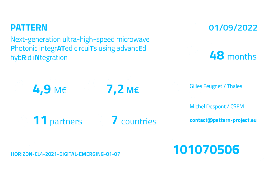
PATTERN is the acronym of the full project title “Next-generation ultra-high-speed microwave Photonic integrATed circuiTs using advancEd hybRid iNtegration”
During its runtime of 4 years, PATTERN will develop the world’s first Process and Assembly Design Kits (PDK & ADK) for microwave photonics at ultra-high frequencies (100+ GHz) as well as new methods of heterogeneous integration of III-V gain materials (e.g. InP) and BiCMOS drivers with electro-optic and nonlinear platforms such as lithium niobate on insulator (LNOI).

Key facts

PATTERN is funded by the EU Research and Innovation Programme Horizon Europe under Grant Agreement No 101070506.
In addition, PATTERN includes partners from the UK, Switzerland and Cyprus, receiving as such funding from UKRI (UK Research and Innovation) and SERI (Swiss State Secretariat for Education, Research and Innovation).

PATTERN aims to
- develop the world’s first PDK and ADK for microwave photonics at ultra‐high frequencies above 100 GHz;
- introduce novel PIC functionalities that currently do not exist, such as magneto‐optic isolators and acousto-optic modulators (AOMs);
- develop new methods for photonic and electronic co-integration;
- cover all PIC foundry process steps, from design and simulation to device fabrication, packaging, and testing;
- showcase the advanced functionalities of the developed PIC prototypes through several demonstrators.
Project datasheet

PATTERN’s vision of an all-in-one chip
PATTERN will integrate all major photonic functionalities on one single hybrid PIC, To this end, PATTERN will:

ENABLE
unrivalled new PIC functionalities, components and subsystems such as fast tuneable lasers for a vast range of applications, from quantum computing and quantum communication to ultra-high-speed telecom, optical computing, sensing and metrology


