NEXT-GENERATION ULTRA-HIGH-SPEED MICROWAVE
Photonic integrATed circuiTs using advancEd hybRid iNtegration
Goals & Objectives
Main Goals
PATTERN addresses many challenges in microwave photonics and PICs at
the same time.
The main project goals are to:
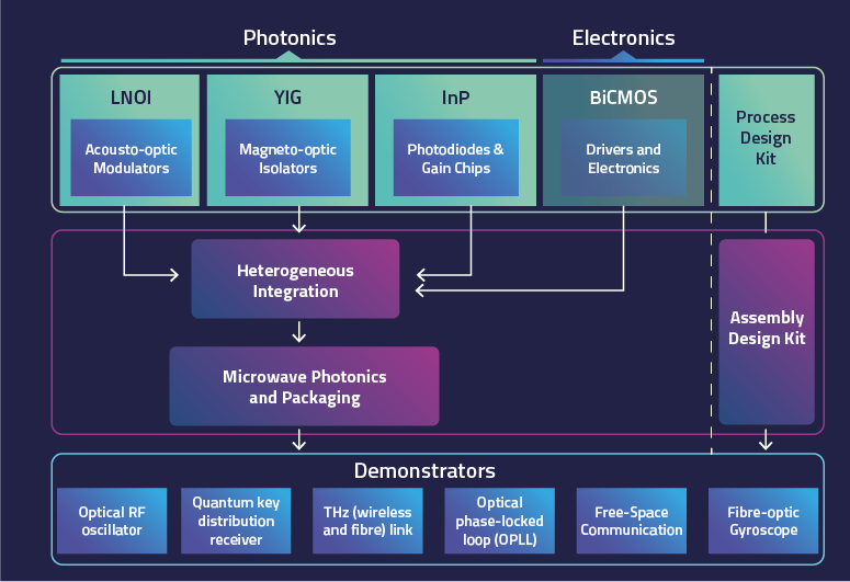
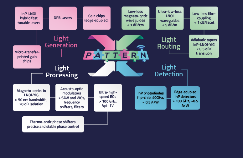
1/ Integrate all major photonic functionalities on a single hybrid PIC: light generation, transmission, manipulation and detection, as well as electronic co-integration.
2/ Pave the way for a new generation of advanced PICs with unrivalled novel functionalities, which will serve a wide range of applications, from telecom and 5G/6G to quantum and optical computing to LiDAR and sensing technologies.

All functions on one chip

PATTERN’s all-in-one PIC platform

PATTERN’s top-level goals translate into five main objectives
- Develop a PIC-scale magneto‐optic isolator based on YIG‐LNOI hybrid integration.
Target: YIG‐LNOI hybrid optical isolator with > 30 dB isolation, < 2 dB insertion losses and > 50 nm of bandwidth. - Develop an AOM based on the combination of surface acoustic waves (SAWs) and a waveguide on an LNOI platform. Target: AOM modulation efficiency of above 6% at maximum speed up to 5 GHz.
- Improve the fabrication of LNOI waveguides to reduce optical losses < 0.05 dB/m. This value represents a four-fold improvement over current CSEM waveguides and can compete with the best state-of-the-art in the literature.
Develop the design flow for the ultra‐high-speed microwave photonic platform based on advanced Building Blocks (BBs), a modelling and chip implementation software and a standardised design kit.
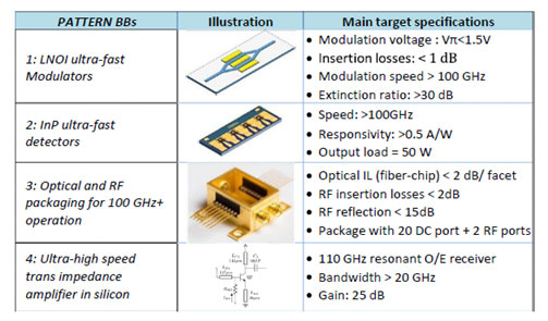
- Develop the world’s first microwave photonics PDK library that includes device models for ultra‐fast LNOI modulators, InP detectors & gain sections, electronic amplifiers, isolators and AOMs in addition to the basic LNOI passive devices (see Table 1)
- Develop modelling capabilities for microwave photonic circuits, predicting circuit behaviour above > 100 GHz
- Develop an ADK library allowing RF electrode routing capabilities for > 100 GHz and design including packaging (with optical and RF interface models).

Table 1: New Building Blocks (BBs) that will be developed under PATTERN
Develop methods and processes for hybrid integration of InP (detectors, gain medium) and Si (electronic RF driver) on top of LNOI based on the following techniques (two techniques each time to mitigate the risks):
- Flip‐chip bonding (lower risk, but series and rather expensive process). Target specifications: < 1 dB / facet optical insertion losses and < 0.5 dB RF losses;
- Micro-Transfer-Printing (higher risk, but parallel and scalable process that should reduce cost). Target specifications: Transfer of up to 50 devices per print, > 80% yield, < 1 dB / facet optical insertion losses and < 0.5 dB RF losses.
Develop a 1550 nm LNOI‐InP fast tunable laser with narrow linewidth.
Targeted specifications:
- Output power > 60 mW
- Linewidth < kHz
- Tuning: 1 ns over 40 nm
Realise six PIC prototypes for the end-user partners in the PATTERN consortium.
The demonstrators address different fields of application, such as microwave photonics and RF-over-fiber, space, inertial sensing, and quantum technologies.
