NEXT-GENERATION ULTRA-HIGH-SPEED MICROWAVE
Photonic integrATed circuiTs using advancEd hybRid iNtegration
INP Platform
Main Advantages
Direct bandgap semiconductor
- Light emission at 1.55 µm
- Light detection at 1.55 µm
Higher electron velocity compared to silicon or gallium arsenide
- Bandwidth of waveguide-integrated photodiodes already achieved > 100 GHz
- Modulator up to 70 GHz
Main weaknesses
- Propagation losses few dB/cm
- PIC density: radius of curvature waveguide > 500µm
Ready for hybrid integration
- Flip-chip with grating couplers on the LNOI chip
- Edge-coupled (multiple die approach )
- Evanescent coupling based on μTP

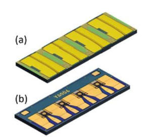
Example of flip-chip-compatible InP gain chips (a) and PD (b) developed by HHI
Beyond the state of art: To realise high-performance InP-on-LNOI devices, e.g. fast narrow linewidth tunable lasers, current InP gain chips and SOAs have to be optimised with regard to low power consumption (low heat dissipation) and efficient optical coupling to LNOI waveguides.
μTP requires optimisation to implement underlying sacrificial layers that allow for a full underetching of the respective InP gain chip and SOA structures.
In PATTERN, HHI’s proven ridge-waveguide-based components will be further developed and optimised for this purpose. New processing steps will be added to the existent InP processing technology. For the InP photodiodes, the design of flip‐chip-compatible surface-illuminated photodiodes needs to be optimised to allow for speeds > 100GHz, while maintaining a sufficiently high responsivity.
