Schematic-assisted design with Luceda IPKISS and CSEM Thin-Film Lithium Niobate (TFLN) PDK
Photonic integrATed circuiTs using advancEd hybRid iNtegration
Schematic-assisted design with Luceda IPKISS and CSEM TFLN PDK

Schematic-assisted design with IPKISS & TFLN PDK
The Horizon Europe PATTERN Project was launched in 2022 to unite the expertise of ten research entities, SMEs, and industrial players in the photonics sector. One of the goals of the PATTERN project is to enable the design of complex microwave photonic circuits, starting from a Process Design Kit (PDK).
A year into the project, PATTERN has made a major stride forward in the design implementation of microwave photonics. This success can be attributed to the development of the CSEM LNOI PDK and advancements in the Luceda Photonics Design Platform, particularly the IPKISS Canvas schematic design environment and IPKISS’ advanced routing capabilities.
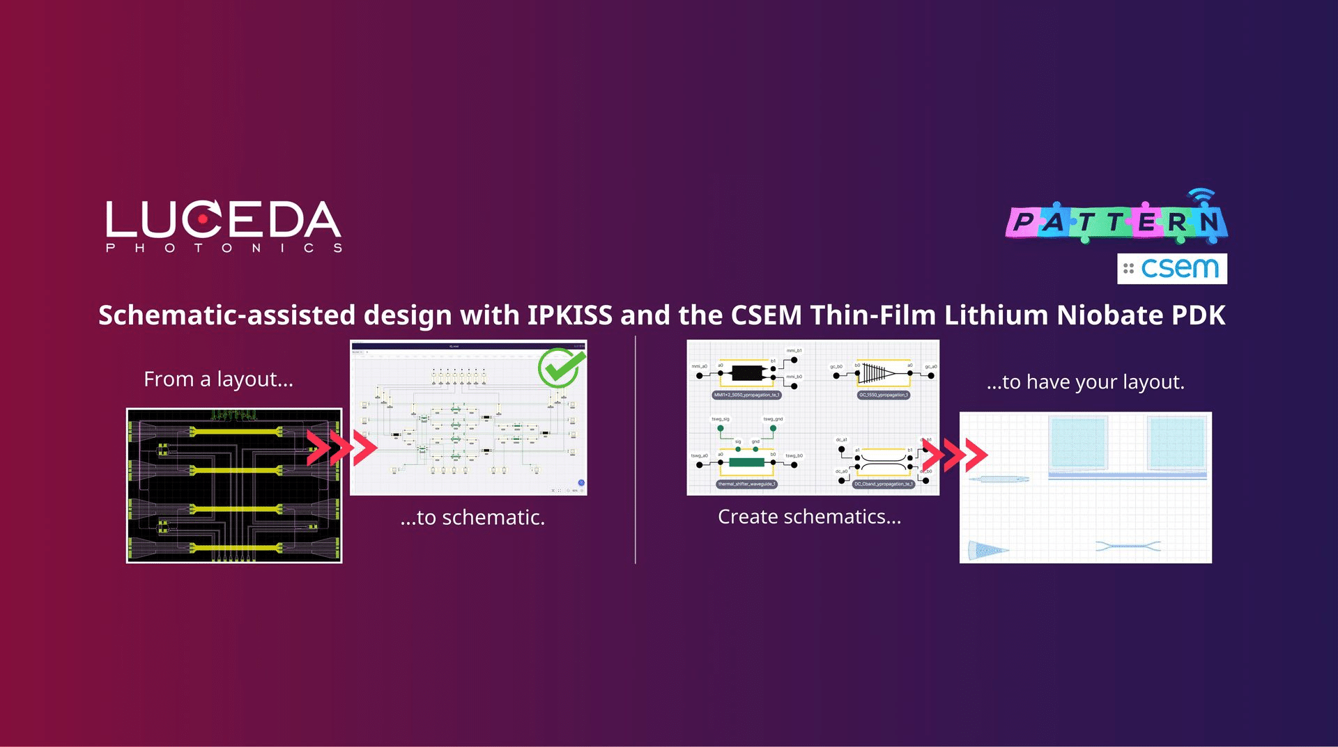
IPKISS Canvas, recently released by Luceda Photonics as part of their flagship product, Luceda IPKISS, empowers designers to swiftly turn new photonic IC circuit ideas into layout implementations. PDK components can be simply dragged and dropped onto the schematic canvas and connected to each other, managing both optical and electrical connectivity. Using code templates, an IPKISS Python script is generated as a starting point for the layout implementation of the PIC. The resulting layout can be validated within the same IPKISS Canvas schematic environment, allowing designers to verify the correctness of the PIC connectivity and device parameters, such as waveguide lengths, in accordance with the conceptual design.
The CSEM Thin-Film Lithium Niobate (TFLN) on Insulator platform PDK, which has been developed as part of the PATTERN and ELENA project efforts, is enabled to work within Luceda IPKISS and IPKISS Canvas. This PDK contains passive components such as splitters, directional couplers, and fiber couplers, and electro-optic components such as high-speed Mach-Zehnder modulators and thermal phase shifters.
In addition to Luceda’s optical and electrical routing automation, the CSEM LNOI PDK now incorporates functionalities for convenient RF trace routing. This includes trace templates, adiabatic transitions and mitered bends.
Finally, designs can be conveniently packaged using an Assembly Design Kit (ADK) developed by Luceda and PHIX. The ADK will greatly streamline the packaging procedure for designers by automatically incorporating alignment loops, fiducial markers, as well as electrical and optical inputs and outputs. When combined with the CSEM LNOI PDK and Luceda IPKISS, this establishes a comprehensive design workflow that spans from concept to tape-out.

