Milestone <2dB per facet fiber-chip coupling
Photonic integrATed circuiTs using advancEd hybRid iNtegration
Key Milestone achieved for facet fiber-chip coupling

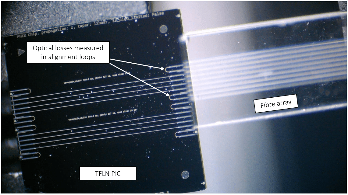
Example of optical edge-coupling process between TFLN PIC and fibre array.
Two waveguide loops are used as an active optical alignment structure.
PHIX report to have successfully achieved a milestone in the PATTERN project by demonstrating fiber-to-chip optical coupling losses of less than 2.0 dB per facet. The milestone has been achieved for a thin film Lithium Niobate (TFLN) on insulator Photonic Integrated Circuit (PIC) designed by Thales and fabricated in a foundry process by CSEM, which got optically edge-coupled to a polarisation-maintaining fibre array (PM FA) manufactured by PHIX.
TFLN PIC waveguides were fabricated with combination of shallow- and fully-etched processes on a 600 nm thin film x-cut 150 mm LNOI wafer. Waveguides were equipped with a standard TFLN PIC platform PDK edge-coupler structure. The edge-coupler’s tapered end was terminated at a tip with 140 nm width, which corresponds to a mode-field diameter of approximately 5.3 µm x 4.7 µm at 1550 nm wavelength (accordingly to numerical simulations conducted by CSEM). Individual PICs got singulated in deep reactive-ion etching (DRIE) process yielding smooth chip facets. Tested chip got fabricated in the second fabrication run in the PATTERN project (named Eiger) during the first half of year 2023.
Polarisation maintaining fibre array was constructed of individual optical fibres spaced by 127.0 µm centre-to-centre pitch. In terms of technical specification, all fibres were spliced sections of Fujikura HA15-PS (mode-field diameter of 4.0 µm at 1550 nm wavelength) joined to Corning PM15 fibres (mode-field diameter of 10.5 µm at 1550 nm wavelength). Fujikura HA15-PS fibre was terminating the fibre array at the interface with the chip, in order to provide a mode-field diameter match with the TFLN PIC waveguides.
PHIX have experimentally measured optical losses via edge-coupling technique using on-PIC alignment loop waveguides. PM FA was utilised to couple and extract optical signals from TFLN PIC. Measurement results revealed a total propagation loop loss of 3.8 dB, resulting in less than 1.9 dB of fiber-chip optical coupling losses per facet. Obtained value satisfies the PATTERN project milestone requirement, where fiber-chip optical coupling losses per facet are required to be lower than 2.0 dB. Total loop propagation loss incorporates several physical phenomena enhancing the losses, namely: splicing loss of individual PM fibres, refractive index mismatch and mode-field diameter mismatch at the interface between measured chip (waveguide) and fibre array (respective optical fibre), propagation loss in the loop due to waveguide bending, core-to-core positional offset of individual fibres in an array structure and others.
Enhancement of optical performance can be achieved by application of an appropriate technical resolution. For this reason, optical facet of the PIC will get mechanically polished by PHIX and refractive index matching liquid (optical adhesive) will be used during optical assembly phase to further decrease coupling losses at the interface between the PIC and the PM fibre array.
This milestone is a big step towards providing a reliable optical interfacing solution for TFLN PICs, which addresses the needs in various application domains. PHIX will report on subsequent achievements and advancements in the PATTERN project.

